GeForce GTX 780 Pictured Some More


It turns out that NVIDIA's upcoming high-end graphics card, the GeForce GTX 780, is indeed based on the GK110 chip, and to the extant of featuring the same reference-design PCB and cooling solution as the GeForce GTX TITAN. Chinese portal IT168 posted press-shots of the card. If you overlook the "GTX 780" embossing on the cooler, half the number of memory chips, and another very subtle difference, you will easily mistake the GTX 780 for a GTX TITAN. 

Pictures reveal the card to feature an ASIC bearing the number "GK110-300-A1," which is rumored to feature 2,304 CUDA cores, 192 TMUs, 48 ROPs, and a 384-bit wide memory interface. Given that the card features just twelve 2 Gbit memory chips, the total memory amount should be 3 GB. The card is said to feature clock speeds of 863 MHz core, 902 MHz GPU Boost, and 6.00 GHz memory, which belts out 288 GB/s memory bandwidth. It draws power from a combination of 6-pin and 8-pin PCIe power connectors. The 4-way SLI-capable card gives out display from a pair of dual-link DVI, HDMI, and DisplayPort connectors.


Source: http://www.techpowerup.com/184202/geforce-gtx-780-pictured-some-more.html

EKWB Intros New GeForce GTX 680 Water Block


EK Water Blocks, Ljubljana based premium water cooling gear provider, is excited to present the EK-FC680 GTX SOC, a new Full Cover (FC) water block for Gigabyte's premium SuperOverclock (GV-N680SO-2GD) edition graphic card.

EK-FC680 GTX SOC is a high performance full-cover water block for engineered specifically for GIGABYTE design GeForce GTX 680 Super OverClock (SOC) series graphics cards. Please check our Cooling Configurator online compatibility system for detailed compatibility list. This water block directly cools the GPU, RAM as well as VRM (voltage regulation module) as water flows directly over these critical areas thus allowing the graphics card and it's VRM to remain stable under high overclocks. EK-FC680 GTX SOC water block also features a very high flow design therefore it can be easily used in liquid cooling systems using weaker water pumps.

Base is made of nickel plated electrolytic copper while the top is made of quality POM Acetal material. The sealing is performed by quality rubber washers. Screw-in brass standoffs are pre-installed and allow for safe, painless installation procedure. Block is mounted with enclosed M3x4 DIN7985 screws and plastic washers.

EK also encloses two-slot I/O bracket which replaces the original three-slot, in order to make installation of mutliple graphics cards easier.

Up to four EK-FC680 GTX SOC series water blocks can be interconnected with EK-FC Bridge & Link system. Additionally this water block lines up with EK-FC680 GTX(+) as well as EK-FC680 GTX FTW series water blocks thus even further expanding users choice of graphics cards. The correct connection link for this water block is already enclosed with the product.

Enclosed: 
- EK-FC680 GTX SOC series water block 
- EK-FC Link
- 2-slot I/O bracket
- mounting mechanism with screw-in brass standoffs
- thermal pads

source: http://www.techpowerup.com/177009/EKWB-Intros-New-GeForce-GTX-680-Water-Block.html

EVGA GeForce GTX 670 FTW LE Detailed


EVGA's high-end air-cooled GeForce GTX 670 FTW graphics card, which launched with the rest of the GTX 670 lineup, is largely based on the GeForce GTX 680 NVIDIA-reference design, including its cooler and PCB, and features clock-speeds of 1006 MHz GPU and 6208 MHz memory. The company recently launched a newer SKU based on the same exact design, the EVGA GTX 670 FTW LE, which goes lighter on the clock speeds. The EVGA GTX 670 FTW LE (model: 02G-P4-2676-KR), features a GPU base clock of 941 MHz, GPU Boost clock of 1019 MHz, and 6008 MHz memory, which is still a notch above NVIDIA-reference speeds. It is priced at US $390.

New Toshiba STT-MRAM Memory Element Promises World's Best Power Consumption


Toshiba Corporation today announced that the company has developed a prototype memory element for a spin transfer torque magnetoresistive random access memory (STT-MRAM) that achieves the world's lowest power consumption yet reported, indicating that it has the potential to surpass the power consumption efficiency of SRAM as cache memory.

Like all digital products, mobile devices, including smartphones and tablet PCs, rely on high-speed memory to supply the main processor with essential instructions and frequently requested data. Until now SRAM has provided the cache-memory solution. However, improving the performance of SRAM to match advances in mobile products results in increasing current leakage, both during operation and in standby mode, degrading power performance.


MRAM, a next-generation memory based on magnetic materials, has emerged as an alternative to SRAM because it is non-volatile, cutting leak current during standby status. However, until now MRAM power consumption has exceeded that of SRAM, throwing up a major barrier to practical application.

Toshiba's new memory element advances the company's pioneering work in STT-MRAM and overcomes the longstanding operating trade-off by securing improved speed while reducing power consumption by 90 percent. The improved structure is based on perpendicular magnetization and takes element miniaturization to below 30 nm. Introduction of this newly designed "normally-off" memory circuit with no passes for current to leak into cuts leak current to zero in both operation and standby without any specific power supply management.

Toshiba has confirmed the performance of the new STT-MRAM memory element with a highly accurate processor simulator. This modeled application of an STT-MRAM integrating the memory as cache memory and recorded a two-thirds reduction in power consumption by a standard mobile chip set carrying out standard operating functions, a result confirming that the new MRAM element has the lowest power consumption yet achieved. This clearly points the way toward the first MRAM with the potential to surpass SRAM in practical operation.

Going forward Toshiba expects to bring the new memory element to STT-MRAM cache memory for mobile processors integrated into smartphones and tablet PCs, and will promote accelerated research and development toward that end.

This work includes results from the "Normally-off Computing" project funded by Japan's NEDO (New Energy and Industrial Technology Development Organization). Toshiba will present three papers on the new STT-MRAM and its technologies on December 11 and 12 at IEDM, the International Electron Device Meeting held by IEEE in San Francisco from December 10.

source: http://www.techpowerup.com/176937/New-Toshiba-STT-MRAM-Memory-Element-Promises-World-s-Best-Power-Consumption.html

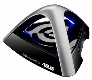
ASUS Introduces the EA-N66 Dual Band Wireless-N900 Gigabit Ethernet Adapter


The ASUS EA-N66 3-in-1 dual band wireless-N900 Gigabit Ethernet adapter is equipped with a unique 3 x 3 patented antenna design, providing users high speed internet access. With selectable dual band operating modes and speeds of up to 450 Mbps per band, the EA-N66 caters to web browsing, smooth HD video streaming, and lag-free online gaming with ease.